Solar
Cell Design and Operation
Solar cells, or photovoltaic (PV) cells
convert electromagnetic energy into electrical energy. Designs of solar-cells have greatly
changed since 1954 when Pearson,
Chapin, and Fuller, researchers at Bell Labs, first reported their discovery of a silicon
solar cell converting 6% of incident sunlight into electricity.
All solar cells work on the same
basic principle: when light strikes the cell it is absorbed by semiconductor layers. A
metallic grid then collects electrons from the semiconductor creating an electric current.
There are two main parts to the cell, an n-type side and a p-type side. The "n"
in n-type stands for negative and means that it has an extra unbonded electron due to the
nature of the doping material, usually phosphorous which has 5 valence electrons in its
outer orbital. The "p" in p-type stands for positive and conversely means that
the doping material, usually boron, has bonds filled by only 3 valence electrons, which
leave "holes."
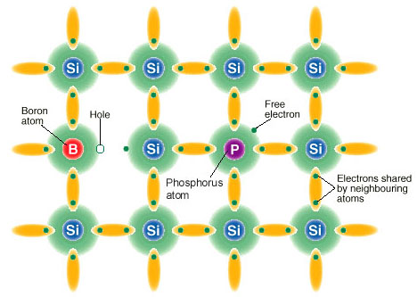
Image courtesy of ACRE - Australian CRC for Renewal Energies
Limited
When these two materials are aligned
opposite to each other, a natural electric field is created as the unbound electrons in
the phosphorus rush to fill in the holes left by the boron atoms. As this is happening a
positive charge builds up on the n-plate, and a negative charge builds up on the p-plate.
This electric field causes the plates to have a voltage difference.
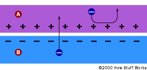

Images courtesy of How Stuff Works
Once electrons build up on the p-type
plate it gets very hard for more electrons to cross the junction. If a photon of light
having sufficient energy, called bandgap energy, strikes an electron on the p-type side,
the electron is knocked free, crosses the gap and collects on the n-plate. An electron
which has crossed the gap is called a photoelectron.
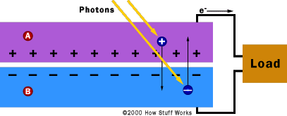
Images courtesy of How Stuff Works
If we connect the cell to an external
circuit, then the photoelectrons will move through that circuit in order to return to the
holes in the p-plate. This process creates a current and does electrical work. The power
of a PV cell is determined by the product of its voltage times the current produced.
PV cells are used in flat plate
collectors or concentrators that can either remain stationary or track the sun's position.
The fundamental types of photovoltaic cells currently in use are single crystalline
silicon, amorphous silicon, and polycrystalline thin films.
Single crystalline silicon cells use
silicon wafers much like those used in electronics, and are therefore rather expensive to
manufacture. These cells are doped with phosphor to make n-type plates and with boron to
make p-type plates. Although expensive, the upside to these cells is that they are the
best semiconductors available.
Amorphous silicon cells are much cheaper
to manufacture than single crystalline silicon cells, but they also have disadvantages.
They do not conduct nearly as well as single crystalline silicon cells, and have many
bonding irregularities which create "holes" on the n-type plate rendering them
less efficient.
Thin film cells are made by applying the
proper materials in layers to a surface, usually glass or plastic. The sequence of
materials is superstrate (opposite of substrate), transparent conductor, n-type layer,
p-type layer, and then a metal conductor to finish the sandwich. These cells are quite
cheap to manufacture but have the disadvantage of not being as efficient as silicon cells.
However, there is a dramatic reduction in the amount of semiconducting material required
and the embedded energy content of the modules in comparison with crystalline
technologies.
Titania cells by Sustainable Technologies
Australia, Ltd. are thin film cells that utilize a revolutionary technology. Instead of
using silicon for the semiconductor they use titanium dioxide impregnated with organic
dyes. This increases the efficiency of the cells since different dyes can be tuned to a
wide variety of band gaps. Titania cells are less dependent on the angle of incidence of
the sun's rays, less sensitive to partial shading, and can operate at a wide range
of temperatures. Titania solar cell manufacture uses non-vacuum processing equipment and
produces no toxic gas emissions.
Another semiconductor at the cutting edge
of solar cell research are those made with gallium arsenide. This very efficient
semi-conductor can be tuned whatever specific voltage the designer needs. The huge
drawbacks are that gallium is more rare than gold, and arsenic is poisonous so
manufacturing these cells is difficult.
Other materials used include gallium
arsenide, copper indium diselenide and cadmium telluride. Since different materials have
different band gaps, they seem to be "tuned" to different wavelengths, or
photons of different energies.
The amount of power drawn from PV cells
depends on their configuration into modules. Most cells produce 0.5
volts, and can be connected in series into modules of 12 volts or higher. One way
efficiency has been improved is to use two or more layers of different
materials with different band gaps. The higher band gap material is on the surface,
absorbing high energy photons while allowing lower energy photons to be absorbed by the
lower band gap material beneath. This technique can result in much higher efficiencies.
The peak wattage depends on the plate's area, the incident radiation's intensity,
frequency, angle of incidence, average average daily insolation (incoming
solar radiation) or ESH
(Equivalent Sun Hours), as well as the ambient temperature and such things as the
air mass above the array, wind, cloudiness, dust and pollution. (email) |