Photonic crystals are dielectric structures which have
bandgaps that prevent certain frequencies of light from passing through them. For this reason we investigated them as the third technical application in Component One.
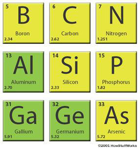
Photonic crystals can be made of
silicon or the elements surrounding it on the periodic table, as shown in this diagram.
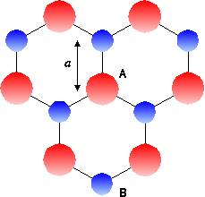
The structure of photonic crystals is like that of graphite, although the material itself is not restricted to graphite. The crystals are
arranged in a hexagonal lattice, as shown in
Fig. 1 below.
The red circles (defined as A) represent Arsenic (As) atoms, and the blue
circles (defined as B) represent Gallium (Ga) atoms, thus forming the graphite (GaAs) lattice structure.
When A sites are occupied by cylinders, a triangular structure is formed. When B sites are occupied
by cylinders of the same type, a
graphite structure is obtained. Essentially, the structure is stretched along an axis into the page to
create cylinders, as shown in Fig. 2 below.
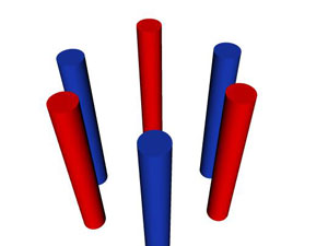
Image courtesy of Sean B and Forrest R
The concept of photonic bandgaps was first introduced in 1987. An array of 1-mm holes were drilled into a slab of material of high refractive index (3.6).
The material,
Yablonovite, named after the scientist performing the experiment, Eli Yablonovitch,
was found to prevent microwaves from propagating in any direction. This
experiment used a one dimensional photonic crystal, which limited light to travel
in one direction, as in Fig. 2 above.
The first way to use photonic crystals is to place them laterally along the length of a surface
with the circumference of the holes
perpendicular to the surface, as shown in Fig. 3 below. Light enters the grating perpendicular to the cylinders, the space between the cylinders limiting
a certain range of wavelengths from passing through.
This is the concept of a one-dimensional photonic crystal, since the light
enters in one direction (perpendicular to the cylinders or into the page) and
leaves in one direction (behind the cylinders).
Fig. 3 Below is an example of a one-dimensional photonic crystal. The
process is similar to Fig. 4: Bright light enters perpendicular to the cylinders from
the front. The contrast between the two dielectric materials (red and blue
cylinders) offsets the blue wavelengths of white light slightly out of phase,
similar to Fig. 4. The constructive interference of
the two blue light waves creates a region of forbidden wavelengths, called a bandgap.
This allows green and red light through to create yellow light, which is less intense to the human eye,
as shown below.
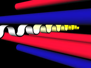
Image courtesy of Sean B.
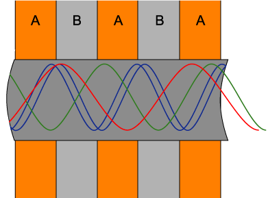
However, photonic crystals can also be used in a much different way. A film of photonic crystals
can be made by
alternating sheets of different dielectric materials into a stack.
Holes are milled through the stack in a hexagonal pattern
to create the photonic crystal sheet. A light wave will pass through different
mediums when it travels through the hole, as shown in Fig. 4 below (a cross section of a photonic crystal viewed from the
side). This is a two-dimensional photonic crystal in a sense
that light travels through the hole, as in Fig. 4, rather than through a group
of cylinders, as in the diagram above. This allows light to enter the hole at an
angle, rather be restricted to a single direction (one dimension), perpendicular
to cylinders.
The reason dielectric material is used to make photonic crystals is that a dielectric has the property to modify a light wave's periodic nature, mainly the amplitude, phase, and
frequency.
When two light waves propagate through a photonic
crystal, one light wave is slightly displaced due to the dielectric's property
to modify the phase of a light wave. The two light waves, slightly out-of-phase,
constructively interfere to create a region of forbidden frequencies, or a gap.
Any other frequency, however, is allowed to pass through. This, succinctly, is
the concept of a bandgap.
Image
courtesy of Daniel W.
The difference between the photonic
crystals in Fig. 3 and Fig. 4 is that the
crystals in Fig. 3 have little to no dielectric material between the
holes, thus forming cylinders in empty space rather than holes in solid
dielectric material.
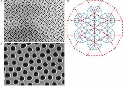
When Fig. 4, photonic crystals are viewed from the top, the view is as shown
in Fig. 5 below. Note the symmetry
of C; the lattice is symmetrical, and thus uniform over the entire sheet.
The size of the cylinders (photonic crystals) in Fig. 2 is on the order of microns.
For the purpose of an application, each graphite cylinder has a diameter of 0.24
microns. This length is larger than 0.9 microns, which is the absolute bandgap
of the near infrared spectrum. Thus, the graphite cylinders have the ability to
prevent the propagation of infrared light, while allowing light of other
wavelengths to pass through. Additionally, the diameter of the graphite
cylinders is large enough not to require the etching of thin dielectric walls,
thus allowing light of other wave lengths to have full intensity. These crystals
can be used in conjunction with other crystals to block out many different
frequencies. The crystals allow all but the unwanted energy to pass through
them.
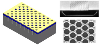
When the photonic crystal sheet in Fig. 4 is stacked, the ending result is a
photonic crystal film ready for application, as shown in the picture below.
 Product